

RGB LED
Multiplexed RGB LED module with analog 4-channel mux and current-limited red, green, and blue channels for the PomeLabs Core Kit.
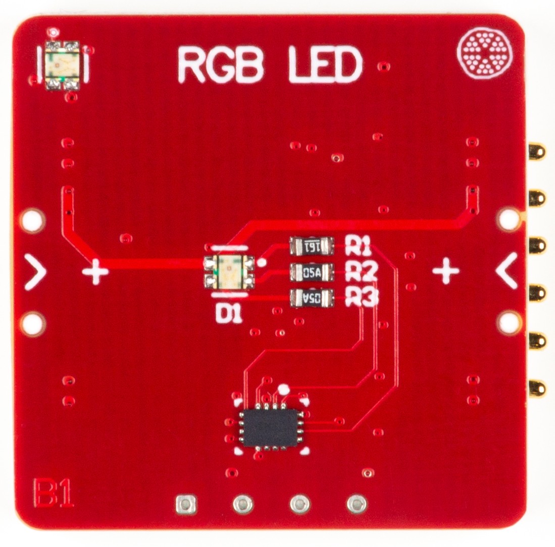
The PomeLabs RGB LED Module (PML-RGB-01) turns three independent light channels — red, green, and blue — into a single controllable color output. A 4-channel analog multiplexer routes Backend MCU signals to each LED channel through precision current-limiting resistors, giving you software-controlled color mixing, brightness modulation, and visual state indication in one compact module.
Revision: v1.0 | Part Number: PML-RGB-01 | Series: PomeLabs Core Kit
Schematic

Digital Twin
In the PomeLabs App, the PML-RGB-01 is mirrored as a digital twin in both the Playground and inside any Connect Activity. On connection the module reports its identity and the App reads its position from the netlist. From the App you can drive the LED colour by switching its three colour channels on or off.
Controls — Parameters You Can Set From the App
Colour channels — Red / Green / Blue · on / off per channel
Toggle each colour channel independently from the App. The three on/off channels combine into eight colours — off, red, green, blue, yellow, magenta, cyan, and white (see the Channel Select Truth Table below). Channels switch fully on or off; the twin does not set intermediate brightness.
Datasheet
1. Overview
The PML-RGB-01 centers on two ICs inside the FE Function block: the LFST-C19H3WT (U1) — a through-hole RGB LED with red, green, and blue emitters in a single package — and the TMUX1511ESVR (U2) — a 4-channel analog multiplexer that routes Backend MCU GPIO signals to the individual LED channels under select-line control.
The architecture separates signal routing from current limiting. U2 handles channel selection via four GPIO-driven select lines (SEL1–SEL4 from GPOUT0–GPOUT3). The current through each LED channel is set by dedicated series resistors: R1 () on the Red channel and R2, R3 ( each) on the Green and Blue channels. The resistor values are chosen to balance perceived brightness across the three emitters given their different forward voltages and luminous efficacy.
2. BOM Components
| Ref. | Type | Value / Part | Role on this module |
|---|---|---|---|
| U1 | RGB LED | LFST-C19H3WT | Single-package RGB LED with separate red, green, and blue emitters. Each emitter driven independently through its own current-limiting resistor. |
| U2 | 4-channel analog multiplexer | TMUX1511ESVR (TI) | Routes Backend MCU GPIO signals to LED channels via select lines SEL1–SEL4. Inputs S1–S4 from MCU; outputs D1–D4 to LED channels. Low on-resistance, wide supply range. |
| R1 | Current-limiting resistor | Series resistor on Red LED channel. Lower value compensates for Red emitter's lower forward voltage — balances perceived brightness. | |
| R2 | Current-limiting resistor | Series resistor on Green LED channel. Limits Green emitter drive current. | |
| R3 | Current-limiting resistor | Series resistor on Blue LED channel. Limits Blue emitter drive current. Identical to R2. | |
| R4 | Resistor | Pull-up resistor on UART lines to . | |
| p1, p2 | Connector | Node headers | Left and Right node connectors exposing , GND, S+, S−, RX/TX, TX/RX. |
3. Electrical Specifications
3.1 U1 — LFST-C19H3WT (RGB LED)
3.1.1 Absolute Maximum Ratings
Exceeding these values may permanently damage the LED. Stress ratings only.
| Parameter | Red | Green | Blue | Unit |
|---|---|---|---|---|
| Forward current () continuous | mA | |||
| Peak forward current (, pulse, duty) | mA | |||
| Reverse voltage () | V | |||
| Power dissipation () | mW | |||
| Operating temperature | to | to | to | °C |
| Storage temperature | to | to | to | °C |
3.1.2 Recommended Operating Conditions
Conditions for reliable operation and optimal performance.
| Parameter | Red | Green | Blue | Unit |
|---|---|---|---|---|
| Forward current () | mA | |||
| Peak forward current (, pulse, duty) | mA | |||
| Operating temperature | to | to | to | °C |
| Forward voltage (, at ) | – | – | – | V |
| Reverse current (, at ) | A | |||
| Luminous intensity (, at ) | – | – | – | mcd |
| Dominant wavelength () | – | – | – | nm |
| Viewing angle () | deg |
3.2 U2 — TMUX1511ESVR (4-Channel Analog Mux)
3.2.1 Absolute Maximum Ratings
Exceeding these values may permanently damage the device. Stress ratings only.
| Parameter | Max Value | Unit |
|---|---|---|
| Supply voltage () | V | |
| Signal voltage on any I/O pin | to | V |
| Select pin voltage | to | V |
| Continuous current per channel | mA | |
| Operating junction temperature () | to | °C |
| Storage temperature () | to | °C |
3.2.2 Recommended Operating Conditions
| Parameter | Min | Typ | Max | Unit |
|---|---|---|---|---|
| Supply voltage () | – | V | ||
| Signal path I/O voltage (source/drain pins) | – | V | ||
| Control input voltage (SELx pins) | – | V | ||
| Ambient temperature () | – | °C | ||
| On-resistance () | – | |||
| On-capacitance () | – | pF | ||
| Off-capacitance () | – | – | pF | |
| Bandwidth | – | – | MHz | |
| (logic input high voltage) | – | – | V | |
| (logic input low voltage) | – | – | V | |
| Input/Output leakage current (ON-state) | – | – | A |
Note: When , the signal path I/O voltage range is limited to –. The device supports input voltages beyond the supply rail, up to (maximum ) when powered within the recommended range.
4. Channel Select Truth Table
SEL1–SEL4 driven by GPOUT0–GPOUT3 from the Backend MCU. Multiple channels can be active simultaneously for color mixing.
| SEL1 (GPOUT0) | SEL2 (GPOUT1) | SEL3 (GPOUT2) | Active Channel | LED Color |
|---|---|---|---|---|
| H | L | L | S1 → D1 → R1 → Red | Red |
| L | H | L | S2 → D2 → R2 → Green | Green |
| L | L | H | S3 → D3 → R3 → Blue | Blue |
| H | H | L | S1 + S2 → Red + Green | Yellow |
| H | L | H | S1 + S3 → Red + Blue | Magenta |
| L | H | H | S2 + S3 → Green + Blue | Cyan |
| H | H | H | S1 + S2 + S3 → All | White |
| L | L | L | None | Off |
5. Pin Descriptions
All signal pins referenced to GND.
| Pin / Net Name | Direction | Description |
|---|---|---|
| GPOUT0 → SEL1 | Input | Select line 1 from Backend MCU. HIGH enables Red channel route through U2 S1→D1→R1→Red LED. |
| GPOUT1 → SEL2 | Input | Select line 2 from Backend MCU. HIGH enables Green channel route through U2 S2→D2→R2→Green LED. |
| GPOUT2 → SEL3 | Input | Select line 3 from Backend MCU. HIGH enables Blue channel route through U2 S3→D3→R3→Blue LED. |
| GPOUT3 → SEL4 | Input | Select line 4 from Backend MCU. Fourth mux channel for auxiliary use. |
| 5V_Module → VDD3 | Power In | supply to U2 VDD and LED anode rail. |
| GND | Ground | Common ground for U2, LED cathodes, and all connectors. |
| TX_L-1 / RX_L-1 | Input / Output | UART Left port. |
| TX_R-2 / RX_R-2 | Input / Output | UART Right port. |
6. Connection Guide & Common Errors
Correct power-up sequence:
- Connect GND first, shared across all modules.
- Connect 5V_Module to a regulated source — this powers both U2 VDD and the LED anode rail.
- Ensure all SEL lines (GPOUT0–GPOUT3) are LOW before power-up to prevent uncontrolled LED activation.
- Drive SEL lines from Backend MCU GPIO outputs. Use PWM for brightness control.
Common wiring errors and consequences:
| Mistake | Symptom | Correction |
|---|---|---|
| SEL lines driven HIGH continuously at full duty cycle | LED overdriven — reduced lifetime, potential permanent damage | Use PWM to control brightness. Recommended duty cycle for continuous operation. |
| 5V_Module supply exceeds | U2 (TMUX1511ESVR) permanently damaged | Keep supply . |
| SEL lines left floating | Random LED activation — undefined mux state | Always drive SEL lines from a defined logic source. Pull to GND if unused. |
| GND not shared with Backend MCU | SEL logic thresholds shift — unreliable channel switching | Ensure a single common GND bus across all modules. |
How is this guide?