

Node Voltage
Protected power switch and relay driver module for the PomeLabs Core Kit.
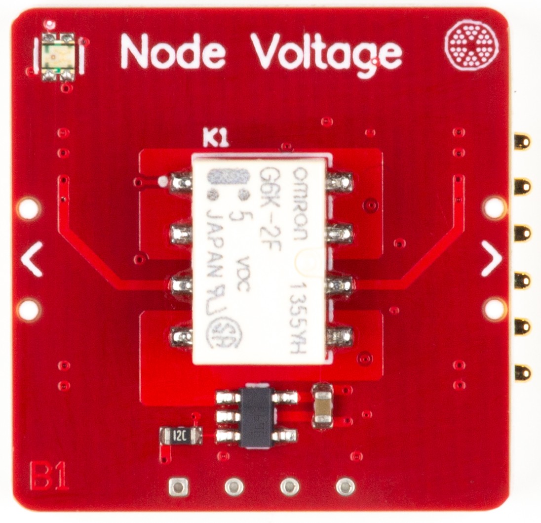
The PomeLabs Node Voltage Module (PML-NV-01) is a multi-function power management module — it controls, protects, and isolates in one board. Plug it in and instantly gain a current-limited power switch and a relay driver with built-in flyback protection, all supervised by your Backend MCU.
Revision: v1.0 | Part Number: PML-NV-01 | Series: PomeLabs Core Kit
Schematic

Digital Twin
In the PomeLabs App, the PML-NV-01 module is mirrored as a digital twin in both the Playground and inside any Connect Activity. On connection the module reports its identity and the App reads its position from the netlist. From the App you can set the module's output level.
Controls — Parameters You Can Set From the App
Output level · toggle, +5 V / GND
Switch the module's output rail between +5 V (VCC) and GND from the App — a single relay set sent over the Connect bus. The underlying power-switch and relay hardware (U1, U2) is described in the Datasheet below.
Datasheet
1. Overview
The PML-NV-01 is organised into two functional layers. The FE Function block contains the active power-management circuitry: U1 (TPS2069EDBVR) is a current-limited, software-controlled USB-class power switch that converts a raw 5V-Module input into a protected 5V-Protected output rail under MCU supervision, while U2 (SZNUD3124LT1G) drives a relay coil (K1) directly from a logic-level GPIO with no external free-wheeling diode required.
This architecture makes the PML-NV-01 the natural bridge between a Backend MCU and any load or node that requires controlled power or galvanic isolation — without any external protection components.
Key characteristics at a glance:
- U1 (TPS2069EDBVR): active-HIGH continuous-current power switch — built-in soft-start, at , output discharge ( typ), reverse-current blocking, deglitched FLT flag ( typ), and typical short-circuit current limit (±20% accuracy)
- U2 (SZNUD3124LT1G): automotive-grade integrated low-side N-MOSFET relay driver — internal Zener clamp ( typ, max), no external free-wheeling diode required, AEC-Q101 qualified, drives relay coils up to at
- K1 (G6K-2F-DC5): coil DPDT signal relay switched by U2, providing galvanic isolation for the load
- FLT fault reporting from U1 to Backend MCU via GPIN0 (open-drain, pulled up through R3 to 3V3)
- C3 () ceramic input bypass capacitor at U1 IN pin per TI application guidelines
- Compatible with all modules in the PomeLabs Core Kit
2. BOM Components
| Ref. | Type | Value / Part | Role on this module |
|---|---|---|---|
| U1 | Power-distribution switch | TPS2069EDBVR (TI) | Primary power switch. N-channel MOSFET with active-HIGH enable. continuous output, typ short-circuit current limit (±20%). Provides built-in soft-start, output discharge ( = typ), reverse-current blocking, fast typ overcurrent response, and typ deglitched FLT reporting. SOT-23-5 (DBV) package, . |
| U2 | Automotive inductive load driver | SZNUD3124LT1G (onsemi) | Integrated N-channel MOSFET relay driver with internal gate-to-drain and gate-to-source resistors plus internal Zener clamp ( = min, typ) — no external free-wheeling diode required. Logic-level gate input ( = –). Drives relay coil K1 up to continuous. AEC-Q101 qualified. SOT-23 (CASE 318) package. Note: marked as DISCONTINUED by onsemi (not recommended for new designs). |
| K1 | Relay | G6K-2F-DC5 (Omron) | DC coil signal relay switched by U2. Provides galvanic isolation between module logic and switched load. Coil energised when GPOUT1 is driven HIGH by Backend MCU. |
| C3 | MLCC bypass capacitor | Input bypass on 5V-Module rail at U1 IN pin. Required per TI TPS2069E application guidelines ( ceramic close to IN/GND for local noise decoupling). | |
| R1, R2 | Resistor | Pull-up resistors on UART TX/RX lines to 3V3. Hold the lines at a defined HIGH idle state when no node is connected. | |
| R3 | Resistor | Pull-up resistor from FLT pin of U1 to 3V3. Required because FLT is open-drain — without this resistor the fault flag cannot present a HIGH idle level. |
3. Electrical Specifications
All values at unless otherwise noted. Specifications from TI SLVSGZ7C (TPS20xxE, Rev. C, March 2025), onsemi NUD3124/D Rev. 15 (SZNUD3124LT1G, June 2024).
3.1 U1 — TPS2069EDBVR
3.1.1 Absolute Maximum Ratings
Exceeding these values may permanently damage the device. Stress ratings only.
| Parameter | Value | Unit |
|---|---|---|
| Input voltage () | to | V |
| Output voltage () | to | V |
| Enable voltage () | to | V |
| FLT pin voltage () | to | V |
| Continuous output current () | Internally limited | — |
| ESD — Human Body Model (HBM) | V | |
| ESD — Charged Device Model (CDM) | V | |
| ESD — IEC 61000-4-2 contact discharge, OUT pin | V | |
| ESD — IEC 61000-4-2 air-gap discharge, OUT pin | V | |
| Junction temperature () | to | °C |
| Storage temperature () | to | °C |
3.1.2 Recommended Operating Conditions
| Parameter | Min | Nom | Max | Unit |
|---|---|---|---|---|
| Input voltage () | V | |||
| Enable input voltage () | — | V | ||
| Enable high-level input voltage () | — | — | V | |
| Enable low-level input voltage () | — | — | V | |
| Continuous output current () | — | — | A | |
| FLT sink current () | — | mA | ||
| Junction temperature () | — | °C | ||
| Ambient operating temperature () | — | °C |
3.1.3 Electrical Characteristics
| Parameter | Min | Typ | Max | Condition |
|---|---|---|---|---|
| at = or | — | — = , over full range | ||
| at = | — | — | — = , = | |
| Output rise time () | — | — = , = , = | ||
| Output fall time () | — | — same conditions as | ||
| Turn-on time () | — | — | — = , = | |
| Turn-off time () | — | — | — same conditions as | |
| Output discharge resistance () | — = = , disabled | |||
| Short-circuit current limit () at | — = , OUT to GND | |||
| Short-circuit current limit () full temp range | — = , OUT to GND | |||
| Overcurrent response time () | — | — | — = , = | |
| Supply current — disabled () at | — | — = | ||
| Supply current — enabled () at | — | — = , = | ||
| UVLO rising threshold | — | — rising | ||
| UVLO hysteresis | — | — | — at | |
| FLT output low voltage () | — | — | — = | |
| FLT off-state leakage | — | — | — = | |
| FLT deglitch time () | — assertion or de-assertion | |||
| Thermal shutdown rising threshold | °C | |||
| Thermal shutdown hysteresis | — | — | °C |
3.2 U2 — SZNUD3124LT1G
3.2.1 Absolute Maximum Ratings
Exceeding these values may permanently damage the device. Stress ratings only.
| Parameter | Value | Unit |
|---|---|---|
| Drain-to-source voltage () — continuous, = | V | |
| Gate-to-source voltage () — continuous, = | V | |
| Drain current () — continuous, = | mA | |
| Single-pulse drain-to-source avalanche energy () | mJ | |
| Peak power dissipation () — square pulse | W | |
| Inductive switching transient () — drain-to-source | V | |
| Reverse battery (), drain-to-source | V | |
| ESD — Human Body Model (HBM) | V | |
| Operating ambient temperature () | to | °C |
| Junction temperature () — max | °C | |
| Storage temperature () | to | °C |
| Total power dissipation — SOT-23, | mW | |
| Thermal resistance junction-to-ambient () — SOT-23 | °C/W |
3.2.2 Electrical Characteristics
| Parameter | Min | Typ | Max | Condition |
|---|---|---|---|---|
| Drain-to-source sustaining voltage () | — = | |||
| Drain-to-source leakage current () | — | — | — = , = , | |
| Gate-body leakage current () | — | — | — = , = , | |
| Gate threshold voltage () | — = , = | |||
| Drain-to-source on-resistance () | — | — | — = , = | |
| Drain-to-source on-resistance () | — | — | — = , = | |
| Output continuous current () | — | — = , = | ||
| High-to-low propagation delay () | — | — | — = , = | |
| Low-to-high propagation delay () | — | — | — same conditions | |
| Rise time () | — | — | — = , = | |
| Fall time () | — | — | — same conditions |
4. Pin Descriptions
All signal pins are referenced to GND.
| Pin / Net Name | Direction | Description |
|---|---|---|
| 5V-Module | Power In | unregulated input supply. Feeds the IN pin of U1. Must be present and stable before EN is asserted. Also drives the K1 relay coil through the U2 low-side switch. |
| 5V-Protected | Power Out | Switched, current-limited output from U1 OUT pin. Active only when GPOUT0 is HIGH. Protected against short circuits and overcurrent ( typ limit, continuous rating). When U1 is disabled, the output is actively discharged through . |
| 3V3 | Power In | logic rail. Supplies the FLT pull-up R3 and the UART pull-ups R1/R2. |
| GPOUT0 | Input | GPIO from Backend MCU. Drives the EN pin of U1. Pull HIGH () to enable 5V-Protected; pull LOW () to disable. Must not be left floating. |
| GPOUT1 | Input | GPIO from Backend MCU. Drives the Gate of U2 through the internal resistor. Drive HIGH ( worst-case to fully turn on) to energise relay coil K1; drive LOW to release the relay. |
| GPIN0 | Output (to MCU) | Open-drain FLT signal from U1, pulled up to 3V3 through R3 (). Active-LOW; asserted during overcurrent or thermal shutdown. The fault is deglitched by typ on both edges. |
| TX_1-L / TX_2-L | Input | UART transmit from Backend MCU (USART1/USART2), routed to the node-side connectors. |
| RX_1-L / RX_2-L | Output | UART receive from node connectors back to Backend MCU. |
| GND | Ground | Common ground reference shared across all ICs, the relay coil return path, and all connectors. |
5. Connection Guide & Common Errors
Correct power-up sequence:
- Connect GND first, ensuring it is shared across the Backend MCU, the PML-NV-01, and any downstream load on the common bus.
- Connect 5V-Module to a regulated source. U1 remains in shutdown (output disabled, output actively discharged through ) until GPOUT0 is asserted HIGH.
- Connect the 3V3 rail. This provides bias for the FLT pull-up R3 and the UART pull-ups R1/R2.
- After both supplies are stable, drive GPOUT0 HIGH to enable 5V-Protected. Soft-start ramps the output in typ ( max at = into / ).
- Drive GPOUT1 HIGH only after the load side is ready. The relay K1 energises in roughly – (typ propagation delay through U2 ; the rest is mechanical).
- Read GPIN0 in firmware to detect FLT events. The signal is debounced internally — a transient overload shorter than (typ) does not assert FLT, and a fault must persist (typ) before GPIN0 goes LOW.
Note on FLT timing: the (–) deglitch window means software cannot rely on FLT to detect very short overcurrent events. Conversely, when clearing a fault by toggling EN, allow the deglitch period to elapse before re-arming the load.
Common wiring errors and consequences:
| Mistake | Symptom | Correction |
|---|---|---|
| EN pin (GPOUT0) left floating | Output state is undefined per TI; charge-pump bias is unstable; 5V-Protected may glitch on or off | Always drive EN actively from GPOUT0. Tie to GND if the rail must be permanently OFF. EN must not be left open per the TI datasheet. |
| FLT pull-up R3 missing or rail floating | FLT line never goes HIGH (it is open-drain) — Backend MCU sees a permanent or floating fault and cannot distinguish good from faulted state | Connect R3 = from FLT to 3V3. 3V3 rail must be live for the pull-up to do its job. |
| Input bypass C3 too small or absent | Local noise/inrush at turn-on causes to dip below the UVLO threshold () — U1 may UVLO-cycle on power-up; long input cables can also drive above the absolute max via inductive overshoot | Place a ceramic capacitor close to IN/GND per TI guideline. For long input cables or noisy supplies, add a – ceramic (or a on OUT) to absorb transients. |
| 5V-Module exceeds (or abs max) | U1 permanently damaged | Keep 5V-Module within the – recommended operating range. Never exceed absolute max. |
| GPOUT1 high level too low for U2 gate | U2 MOSFET does not fully enhance — high , relay may not pull in cleanly, MOSFET dissipates excessive power | is min / max. Drive GPOUT1 to guarantee full enhancement; is ideal. The internal + network leaves the MOSFET OFF when GPOUT1 floats. |
| Free-wheeling diode added across K1 coil externally | Inductive kickback bypasses the U2 internal Zener clamp, slowing relay drop-out and partially defeating the integrated solution | U2's internal Zener clamp ( = min, typ) absorbs the kickback by design — no external free-wheeling diode is required or recommended. |
| Relay coil current exceeds | U2 rating exceeded; thermal stress on the SOT-23 ( max dissipation) | Verify the K1 coil current at the operating supply voltage. The G6K-2F-DC5 has a coil resistance well above , keeping well within spec. |
| 5V-Module and 5V-Protected shorted together externally | Bypasses U1's short-circuit protection — the upstream supply sees the load directly with no current limit | Keep 5V-Module and 5V-Protected as separate nets. Only U1 bridges them. |
| Reading FLT immediately after enabling U1 | False fault reported during the soft-start window | FLT is high-impedance during UVLO, and the deglitch may not have settled. Wait at least after asserting EN before sampling GPIN0. |
| Designing a new product around U2 | SZNUD3124LT1G is marked "DISCONTINUED — not recommended for new design" by onsemi (NUD3124/D Rev. 15) | For new designs, contact onsemi for a recommended replacement (e.g. NCV8402 series or a discrete logic-level MOSFET + flyback diode). The PML-NV-01 retains the part for legacy compatibility only. |
How is this guide?