

Probe
Dual-channel 1Ω shunt probe module for simultaneous current and voltage measurement for the PomeLabs Core Kit.
The PomeLabs Probe Module (PML-PR-01) puts precision measurement directly into the signal path. Two calibrated shunt resistors sit in-line on the S+ and S− channels simultaneously — measure the voltage drop across either shunt and you have the current; measure either terminal to ground and you have the node voltage. One module, two channels, non-intrusive, always live.
Revision: v1.0 | Part Number: PML-PR-01 | Series: PomeLabs Core Kit
Schematic

Digital Twin
In the PomeLabs App, the PML-PR-01 is mirrored as a digital twin in both the Playground and inside any Connect Activity. On connection the module reports its unique ID, firmware version, and type, and the App places it in your circuit by reading the live netlist — so you always see which module it is and how it is wired. The Probe inserts two precision shunts as a measurement point: the differential voltage across them is captured through the Scope instrument, not streamed by the Probe twin itself, so the current release exposes no app-side controls or streamed values for this module.
Datasheet
1. Overview
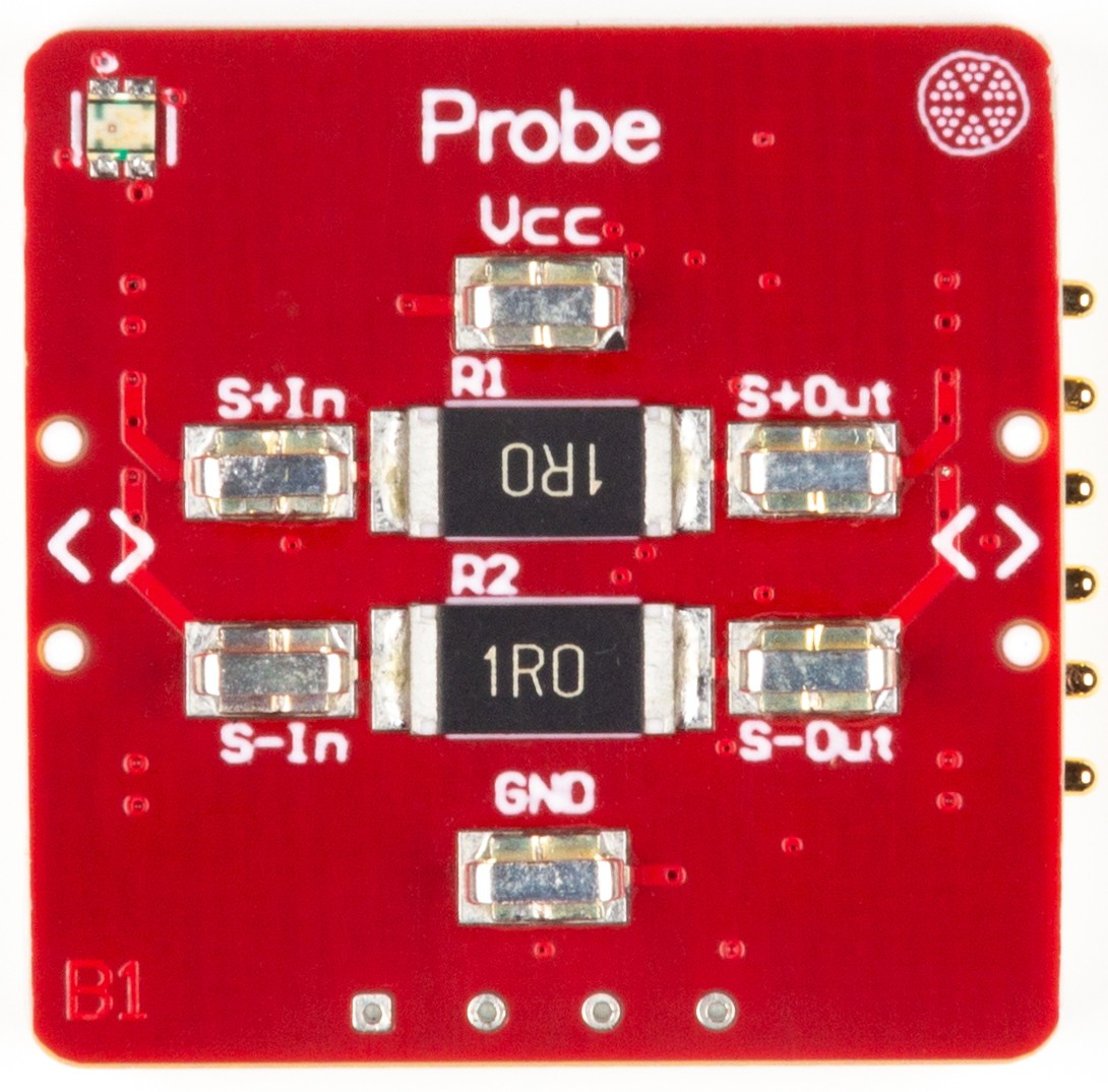
The PML-PR-01 inserts two precision thick-film shunt resistors (R1 and R2, ERJ-1TRQF1R0U) in series with the S+ and S− signal paths respectively. The resistors are placed inside the FE Function block between Pogo-connector measurement points (S+_In / S+_Out and S-_In / S-_Out), allowing a Backend MCU or external instrument to measure the differential voltage across each shunt and derive the instantaneous current with a simple Ohm's law calculation.
At and continuous power rating, each shunt can carry up to continuously () before reaching its thermal limit, making it suitable for measuring signal-level and low-power load currents across the full PomeLabs Core Kit range. The resistor tolerance and temperature coefficient ensure measurement accuracy is dominated by the ADC resolution of the Backend MCU rather than the shunt itself across the full to operating range.
2. BOM Components
| Ref. | Type | Value / Part | Role on this module |
|---|---|---|---|
| R1 | Thick-film shunt resistor | ERJ-1TRQF1R0U (Panasonic) | , , , . Inserted in series on the S+ signal path inside the FE Function block. Voltage drop across R1 = current in S+ channel . 2512 SMD package. |
| R2 | Thick-film shunt resistor | ERJ-1TRQF1R0U (Panasonic) | , , , . Inserted in series on the S− signal path inside the FE Function block. Identical to R1. |
| Vcc | Connector | RH-5019 | 5V_Module power input connector. Supplies the module Vcc rail. |
| GND1, GND2 | Connector | RH-5019 | Left and Right ground reference connectors inside the FE Function block. |
| S+_In, S+_Out | Connector | RH-5019 | Input and output measurement points on the S+ channel, flanking R1. |
| S-_In, S-_Out | Connector | RH-5019 | Input and output measurement points on the S− channel, flanking R2. |
| p1, p2 | Connector | Node headers | Left and Right node connectors exposing +5V, GND, S+, S−, RX/TX, TX/RX to downstream modules. |
3. Electrical Specifications
Shunt specifications from Panasonic ERJ-1TRQF1R0U datasheet.
3.1 Shunt Resistors (ERJ-1TRQF1R0U)
3.1.1 Absolute Maximum Ratings
Exceeding these values may permanently damage the shunt. Stress ratings only.
| Parameter | Max Value | Unit |
|---|---|---|
| Continuous power dissipation () | W | |
| Continuous current at ( @ = , = ) | A | |
| Operating temperature | to | °C |
| Storage temperature | to | °C |
| Short-time overload ( pulse, ) | W |
3.1.2 Recommended Operating Conditions
| Parameter | Recommended Range | Unit |
|---|---|---|
| Continuous current | to | A |
| Ambient operating temperature | to | °C |
| Differential measurement voltage | V | |
| Recommended ADC resolution | bits |
3.2 Probe Connector — RH-5019
3.2.1 Absolute Maximum Ratings
| Parameter | Value | Unit |
|---|---|---|
| Maximum voltage | TBD | V |
| Maximum current per pin | TBD | A |
| Operating temperature | TBD | °C |
3.2.2 Recommended Operating Conditions
| Parameter | Recommended Value | Unit |
|---|---|---|
| Recommended insertion cycles | TBD | cycles |
| Contact resistance | TBD | |
| Recommended operating voltage | V |
4. Pin Descriptions
All signal pins are referenced to GND.
| Pin / Net Name | Direction | Description |
|---|---|---|
| S+_L | Input | S+ signal input from the Left node connector. Enters the FE Function block and feeds S+_In / R1. |
| S+_R | Output | S+ signal output to the Right node connector. Exits the FE Function block from S+_Out / R1. |
| S-_L | Input | S− signal input from the Left node connector. Enters the FE Function block and feeds S-_In / R2. |
| S-_R | Output | S− signal output to the Right node connector. Exits the FE Function block from S-_Out / R2. |
| S+_In | Measurement point | Upstream terminal of R1. Connect ADC input here for differential current measurement on S+ channel. |
| S+_Out | Measurement point | Downstream terminal of R1. Connect second ADC input here for differential measurement. |
| S-_In | Measurement point | Upstream terminal of R2. Connect ADC input here for differential current measurement on S− channel. |
| S-_Out | Measurement point | Downstream terminal of R2. Connect second ADC input here for differential measurement. |
| 5V_Module | Power In | supply input. Powers module Vcc rail via RH-5019 connector. |
| GND1, GND2 | Ground | Left and Right ground references inside the FE Function block. Both connect to the common GND bus. |
| TX_L-1 / RX_L-1 | Input / Output | UART transmit and receive — Left port. |
| TX_R-2 / RX_R-2 | Input / Output | UART transmit and receive — Right port. |
5. Connection Guide & Common Errors
Correct connection sequence:
- Connect GND to the common ground bus shared across all modules.
- Connect 5V_Module to a regulated source.
- Insert the Probe Module in series with the signal path — S+_L / S-_L to the source, S+_R / S-_R to the load.
- Connect Backend MCU ADC inputs to the measurement point pairs: S+_In and S+_Out for S+ current, S-_In and S-_Out for S− current.
- Use differential ADC mode or subtract two single-ended readings to obtain .
- Apply to convert voltage to current.
Common wiring errors and consequences:
| Mistake | Symptom | Correction |
|---|---|---|
| Current through shunt exceeds continuously | Shunt self-heats beyond rated power (); resistance drifts then device fails | Keep continuous current . For higher currents, use an external lower-value shunt. |
| Measuring single-ended voltage at S+_Out only | Reading includes both shunt drop and source voltage — current calculation incorrect | Always measure differential: . Use a differential ADC or instrumentation amplifier. |
| GND reference not shared with measurement instrument | Common-mode voltage causes ADC input to exceed rail, corrupts reading or damages ADC | Ensure ADC GND and module GND are on the same bus. |
| Probe inserted in wrong direction (input and output swapped) | Differential voltage reads negative — negative current result | Verify S+_L connects to signal source and S+_R connects to load. |
| High-impedance signal source loaded by shunt | Signal voltage droops under load | is appropriate for low-impedance sources only. Do not use on high-impedance voltage sources. |
How is this guide?