

XOR Gate
3-state 2-input XOR gate with Schmitt-trigger inputs for the PomeLabs Core Kit.
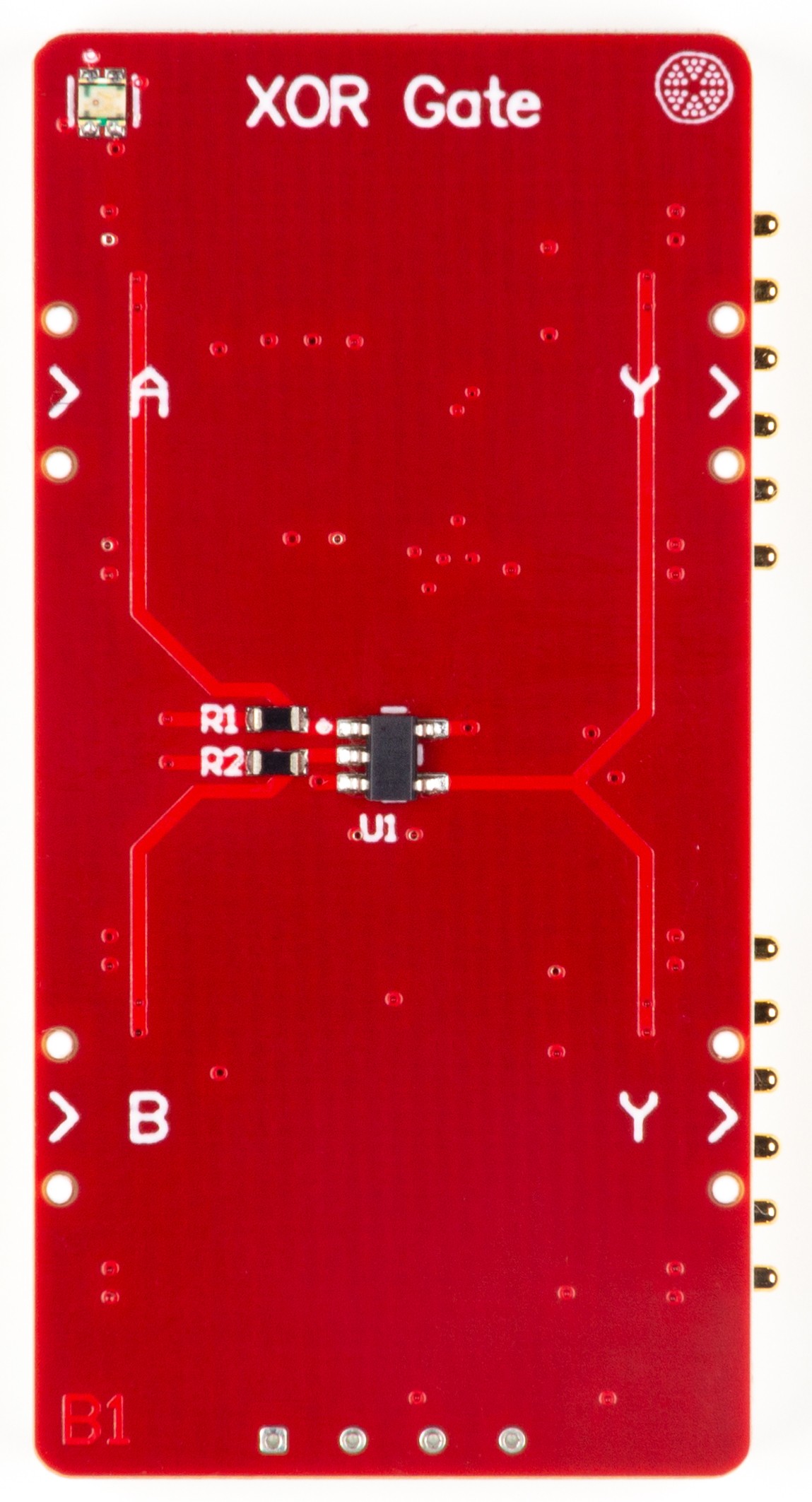
The PomeLabs XOR Gate Module (PML-XG-01) captures one of the most useful and counterintuitive operations in digital logic — output HIGH when inputs disagree, LOW when they match. It is the foundation of binary addition, parity checking, and controlled inversion. Built on the same configurable IC as the AND and NOT Gate Modules, it demonstrates how three entirely different logic behaviors emerge from the same silicon through configuration alone.
Revision: v1.0 | Part Number: PML-XG-01 | Series: PomeLabs Core Kit
Schematic

Digital Twin
In the PomeLabs App, the PML-XG-01 is mirrored as a digital twin in both the Playground and inside any Connect Activity. On connection the module reports its unique ID, firmware version, and type, and the App places it in your circuit by reading the live netlist — so you always see which module it is and how it is wired. Its combinational logic runs entirely on the physical gate IC; the current release exposes no app-side controls or streamed values for this module.
Datasheet
1. Overview
The PML-XG-01 implements a 2-input Exclusive-OR gate using the SN74LVC1G99DCUR (U1) — the same ultra-configurable gate used in the AND and NOT Gate Modules, here configured as a 3-state XOR. OE is permanently tied LOW.
Output Y is HIGH only when inputs A (S+_UL) and B (S+_LL) differ from each other. When both inputs are the same — both LOW or both HIGH — output Y is LOW. Y drives both S+_UR and S+_LR simultaneously. The XOR configuration is unique within the SN74LVC1G99 function table: input B is routed to configuration pin D rather than a dedicated input, making it the most instructive configuration to compare against AND and NOT when studying how programmable logic works.
2. BOM Components
| Ref. | Type | Value / Part | Role on this module |
|---|---|---|---|
| U1 | Configurable logic gate | SN74LVC1G99DCUR (TI) | Configured as 3-state XOR: C = L, D = Input 2 (B), OE = GND. Schmitt-trigger inputs ( hysteresis typ at ). SC-70-8 (DCUR) package. |
| R1, R2 | Resistor | Pull-up resistors on UART TX/RX lines to . | |
| p1–p4 | Connector | Node headers | Four node connectors exposing , GND, S+, S−, RX/TX, TX/RX to downstream modules. |
3. Electrical Specifications
All values at unless otherwise noted. Gate specifications from TI SCES609G (SN74LVC1G99, Rev. G, Nov 2013).
3.1 U1 — SN74LVC1G99DCUR
3.1.1 Absolute Maximum Ratings
Exceeding these values may permanently damage the device. Stress ratings only.
| Parameter | Max Value | Unit |
|---|---|---|
| Supply voltage () | to | V |
| Input voltage () | to | V |
| Output voltage — high-Z or power-off state () | to | V |
| Output voltage — high or low state () | to | V |
| Input clamp current () | mA | |
| Output clamp current () | mA | |
| Continuous output current () | mA | |
| Continuous current through or GND | mA | |
| Thermal impedance — DCU package | °C/W | |
| Storage temperature () | to | °C |
3.1.2 Recommended Operating Conditions
| Parameter | Min | Max | Unit / Notes |
|---|---|---|---|
| Supply voltage () — operating | V | ||
| Input voltage () | V — inputs accept up to regardless of | ||
| Output voltage () | V | ||
| High-level output current () @ | — | mA (sourcing) | |
| Low-level output current () @ | — | mA (sinking) | |
| High-level output current () @ | — | mA (sourcing) | |
| Low-level output current () @ | — | mA (sinking) | |
| Operating temperature () | °C |
4. Truth Table
| OE | A (S+_UL) | B (S+_LL) | Y Output (S+_UR / S+_LR) |
|---|---|---|---|
| L | L | L | L — inputs identical (both LOW), output LOW |
| L | L | H | H — inputs differ, output HIGH |
| L | H | L | H — inputs differ, output HIGH |
| L | H | H | L — inputs identical (both HIGH), output LOW |
| H | X | X | Z — output disabled (high impedance) |
5. Pin Descriptions
All signal pins are referenced to GND.
| Pin / Net Name | Direction | Description |
|---|---|---|
| S+_UL | Input | Logic input A to U1. Upper-Left signal — first XOR input. Y HIGH when this differs from B. |
| S+_LL | Input | Logic input B to U1. Lower-Left signal — second XOR input. Y HIGH when this differs from A. |
| S+_UR / S+_LR | Output | XOR output Y. HIGH when inputs differ; LOW when identical. Drives both output channels simultaneously. |
| TX_UL-L / TX_LL-L | Input | UART transmit from Backend MCU (USART1/USART3). |
| RX_UL-L / RX_LL-L | Output | UART receive from Upper-Left and Lower-Left connectors. |
| TX_UR-L / TX_LR-L | Input | UART transmit from Backend MCU (USART2/USART4). |
| RX_UR-L / RX_LR-L | Output | UART receive from Upper-Right and Lower-Right connectors. |
| 5V-Module | Power In | supply. Powers of U1. |
| 3V3 | Power In | logic rail for pull-up resistors R1–R2 (). |
| GND | Ground | Common ground for all ICs and connectors. |
6. Connection Guide & Common Errors
Correct power-up sequence:
- Connect GND first, shared across all modules on the common bus.
- Connect 5V-Module to a regulated source to power U1.
- Connect 3V3 rail for UART pull-up resistors.
- Verify OE is LOW (tied to GND on this module) — output should be active.
- Apply logic signals to S+_UL and S+_LL and observe output on S+_UR / S+_LR.
Common wiring errors and consequences:
| Mistake | Symptom | Correction |
|---|---|---|
| OE left floating on U1 | Output enters high-Z randomly | Tie OE to GND. Never leave floating. |
| Input A or B left floating | Undefined input — XOR output unpredictable | Always drive both S+_UL (A) and S+_LL (B) from defined logic sources. |
| to U1 exceeds | U1 permanently damaged | Keep . |
| Input signal exceeds | Clamp current flows; damage if | Add series resistor if overvoltage risk exists. |
| Output Y driving load | Current limit exceeded | Keep within . |
| Confusing XOR with XNOR | Y LOW when inputs differ — opposite of expected | XOR: Y HIGH when inputs differ. XNOR: Y HIGH when inputs identical. Verify configuration pins. |
How is this guide?