

OpAmp
Datasheet and digital-twin reference for the PML-OA-01 Operational Amplifier module.
The PomeLabs Op-Amp Module (PML-OA-01) is a snap-together analog building block that brings the full power of a precision operational amplifier into the PomeLabs ecosystem — no breadboard, no wiring errors, just connect and experiment.
Revision: v1.0 | Part Number: PML-OA-01 | Series: PomeLabs Core Kit
Schematic

Digital Twin
In the PomeLabs App, the PML-OA-01 module is mirrored as a digital twin in both the Playground (free-form circuit sandbox) and inside any Connect Activity (guided lab). On connection the module reports its unique ID, firmware version, and type, and the App places it in your circuit by reading the live netlist — so you always see which module it is and how it is wired. Its analog behaviour runs entirely on the physical hardware; the current release exposes no app-side controls or streamed values for this module.
Datasheet
1. Overview
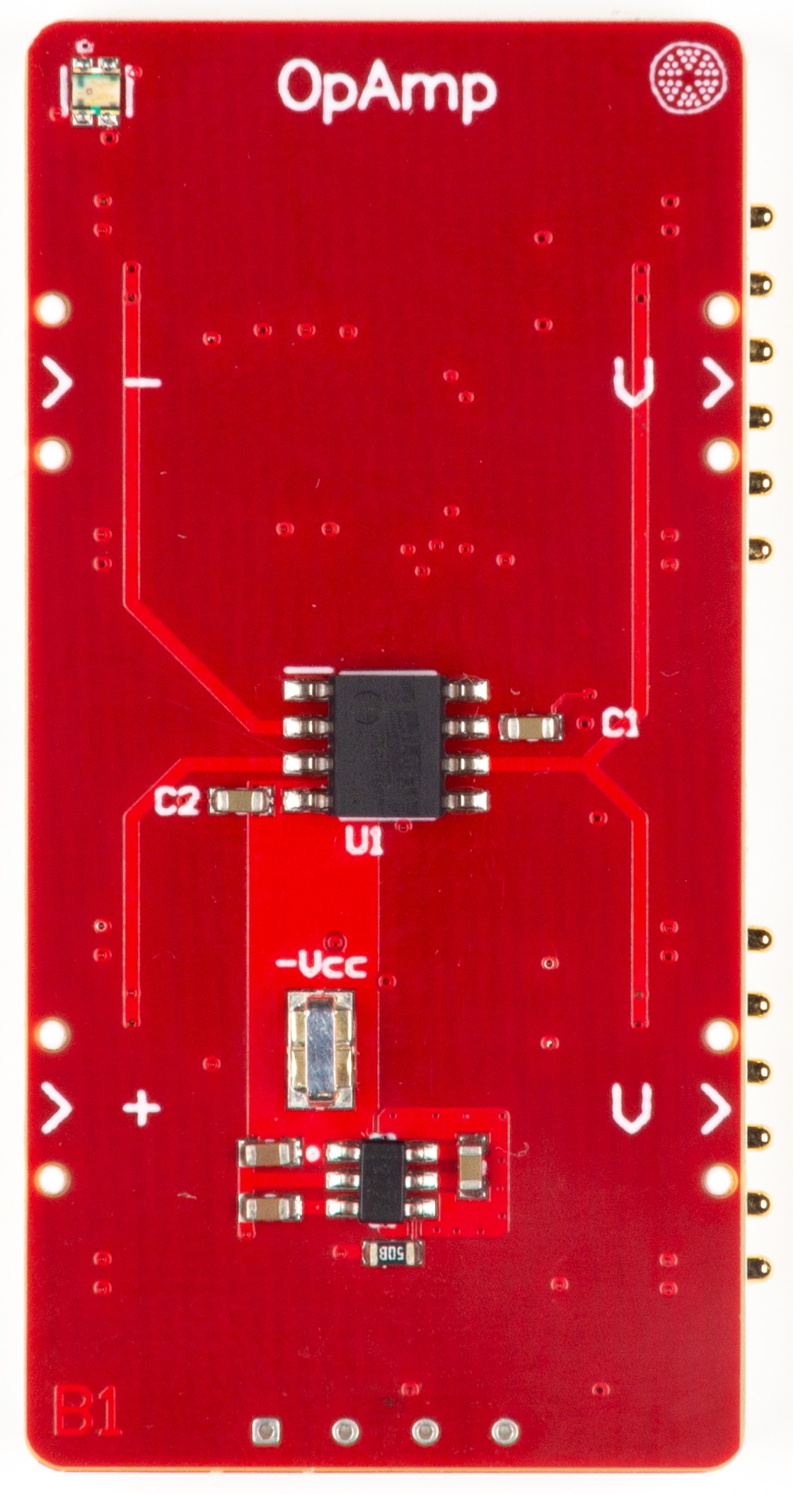
The PML-OA-01 centers on a TL081HIDR JFET-input operational amplifier (U1), chosen for its gain-bandwidth product, slew rate, and sub- input offset — performance characteristics that make it suitable for audio, instrumentation, and control circuit experiments at the educational level. A key design decision is the onboard LM2776DBVR switched-capacitor voltage inverter (U2), which generates a mirrored negative rail from a single supply at up to and switching frequency. This eliminates the dual-rail bench supply typically required for op-amp circuits, significantly reducing setup complexity in classroom environments. All ten signal and power pins, including the inverting and non-inverting inputs, output, VCC, GND, VEE, and the U2 enable line (EN), are exposed through labeled header connectors that map directly to the module pinout diagram. The module supports any standard single op-amp topology: inverting and non-inverting amplifiers, voltage followers, comparators, differentiators, and integrators — all configurable with external passive components from the PomeLabs Core Kit.
2. BOM Components
| Ref. | Type | Value / Part | Role on This Module |
|---|---|---|---|
| U1 | JFET-input op amp | TL081HIDR (TI) | Core signal amplification IC. Single-channel, slew rate, GBW FET-input op amp in 8-pin SOIC. TL08xH grade: to , integrated EMI/RF filters. |
| U2 | Switched-cap voltage inverter | LM2776DBVR (TI) | Charge-pump inverter converting positive VCC to mirrored negative rail () at up to . switching, efficiency. SOT-23-6 (DBV) package. |
| C1, C2 | MLCC decoupling | ceramic | Decoupling capacitors on U2 supply rails. X7R or X5R; voltage rating . |
| C3, C4 | MLCC decoupling | ceramic | Input (CIN) and flying (C1) capacitors for the LM2776DBVR charge pump. Low-ESR X7R or X5R preferred. |
| C5 | MLCC decoupling | ceramic | Output capacitor (COUT) for U2. Low-ESR ceramic minimizes ripple. |
| RH-5019 | Test point / connector | Ref. designator | Negative rail () measurement or inter-module chaining point at VOUT of U2. |
3. Electrical Specifications
All values at unless otherwise noted. Specifications from TI SLOS081O (TL081HIDR, Rev. O) and TI SNVSA56B (LM2776DBVR, Rev. B).
3.1 TL081 (U1)
3.1.1 Absolute Maximum Ratings
Exceeding these values may permanently damage the module. Stress ratings only.
| Parameter | Symbol | Max Value | Unit |
|---|---|---|---|
| Supply voltage () | ( operating) | V | |
| Common-mode input voltage | to | V | |
| Differential input voltage | (clamped) | V | |
| Input signal current | mA | ||
| Output short-circuit duration | Continuous (1 ch at a time) | — | |
| Operating junction temperature | °C | ||
| Storage temperature | to | °C |
3.1.2 Recommended Operating Conditions
| Parameter | Min | Typical | Max | Unit |
|---|---|---|---|---|
| Op-amp supply voltage range | V | |||
| Input signal frequency range | DC | — | GBW | — |
| Quiescent current (per channel) | — | — | µA | |
| Gain-bandwidth product (GBW) | — | — | MHz | |
| Slew rate | — | — | V/µs | |
| Open-loop voltage gain () | — | dB | ||
| Input offset voltage | — | mV | ||
| Input offset voltage drift | — | — | µV/°C | |
| CMRR | — | dB | ||
| PSRR | — | µV/V | ||
| Input bias current | — | pA | ||
| Input voltage noise density () | — | — | ||
| THD | — | — | % | |
| Operating temperature (ambient) | °C |
3.2 LM2776 (U2)
3.2.1 Absolute Maximum Ratings
Exceeding these values may permanently damage the module. Stress ratings only.
| Parameter | Symbol | Max Value | Unit |
|---|---|---|---|
| Output current limit (short-circuit) | mA | ||
| UVLO threshold falling | V | ||
| Thermal shutdown junction temperature | °C |
3.2.2 Recommended Operating Conditions
| Parameter | Min | Typical | Max | Unit |
|---|---|---|---|---|
| Input voltage (, VCC pin) | V | |||
| Internal positive rail (post-U2) | — | — | V | |
| Internal negative rail (post-U2) | — | — | V | |
| Output current (continuous, to U1 supply) | — | mA | ||
| Quiescent supply current (, EN = 1, no load) | — | µA | ||
| Shutdown supply current (, EN = 0) | — | µA | ||
| Switching frequency () | MHz | |||
| Output resistance () | — | — | Ω | |
| EN threshold — enable (active-high) | — | — | V | |
| EN threshold — shutdown | — | — | V | |
| UVLO threshold rising | — | — | V | |
| Package | — | SOT-23-6 (DBV), | — | — |
4. Pin Descriptions
The module exposes ten labeled pins. All signal pins are referenced to GND.
| Pin Name | Channel | Direction | Description |
|---|---|---|---|
| S+_UL | Upper | Input | Non-inverting input () of the upper op-amp channel. Connect signal to be amplified in-phase. |
| S+_UR | Upper | Output | Output of the upper op-amp channel. Drive loads . Do not short to GND. |
| S+_LL | Lower | Input | Non-inverting input () of the lower op-amp channel. |
| S+_LR | Lower | Output | Output of the lower op-amp channel. Drive loads . Do not short to GND. |
| VCC | Both | Power In | Positive supply input to LM2776DBVR charge-pump inverter. Apply DC. |
| VEE / −Vcc | Both | Power Out | Negative rail generated internally by U2 (). Measurement only. Do not drive externally. |
| GND | Both | Ground | Common ground reference. Connect before any signal or power pins. |
| EN | Both | Input | Enable control for U2 (LM2776DBVR). Pull HIGH for normal operation; pull LOW for shutdown. |
Correct power-up sequence:
- Connect GND first to the common ground bus.
- Connect VCC to a regulated DC source (; recommended for classroom use).
- Verify EN pin is HIGH (or tie to VCC) to enable U2.
- Verify −Vcc pin reads approximately before connecting signal pins.
- Connect signal inputs (S+_UL / S-_UL) only after power is stable.
Common wiring errors and consequences:
| Mistake | Symptom | Correction |
|---|---|---|
| VCC out-of-range ( to U2) | U2 may enter thermal shutdown or be permanently damaged | Keep VCC for U2. If higher supply needed, add pre-regulator. |
| EN pin left floating | U2 may not start or behaves unpredictably | Tie EN HIGH (to VCC) for always-on mode, or control via GPIO. Pull to GND for shutdown. |
| Input floating (S+ or S−) | Output saturates to or oscillates | Connect both inputs. Use resistor to GND on unused inputs. |
| Driving −Vcc / VEE from external source | U2 permanently damaged; may damage U1 | VEE / −Vcc is an output only. Never apply external voltage to this pin. |
| Load resistance on OUT pin | Reduced output swing, distortion | Drive loads . |
| Input signal beyond range | Clipped output; possible latch-up | Keep signal inputs within to . Add input protection resistor. |
| C3/C4/C5 wrong type (Y5V/Z5U ceramic) | U2 output ripple high, efficiency reduced | Use X7R or X5R MLCCs. Y5V/Z5U lose capacitance under DC bias. |
© PomeLabs. All rights reserved. Specifications subject to change without notice.
How is this guide?