

OR Gate
Dedicated fixed-function 2-input OR gate for the PomeLabs Core Kit.
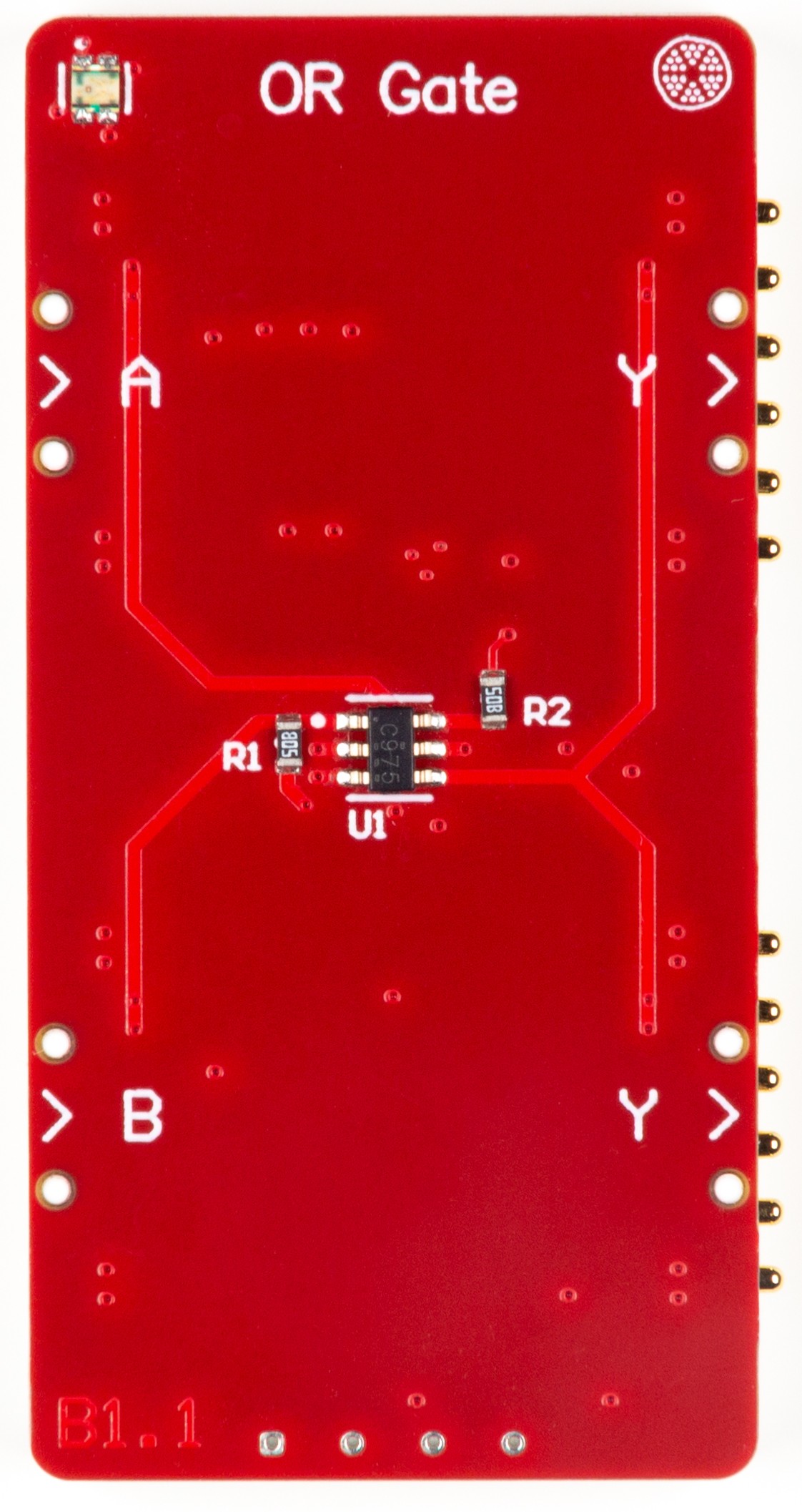
The PomeLabs OR Gate Module (PML-OG-01) is the kit's most permissive logic gate — output HIGH the moment either input goes HIGH, LOW only when both go silent simultaneously. Unlike the configurable IC behind the AND, NOT, and XOR modules, this one uses a dedicated, fixed-function OR gate: no configuration pins, no ambiguity, just of clean positive-OR logic from to .
Revision: v1.0 | Part Number: PML-OG-01 | Series: PomeLabs Core Kit
Schematic

Digital Twin
In the PomeLabs App, the PML-OG-01 is mirrored as a digital twin in both the Playground and inside any Connect Activity. On connection the module reports its unique ID, firmware version, and type, and the App places it in your circuit by reading the live netlist — so you always see which module it is and how it is wired. Its combinational logic runs entirely on the physical gate IC; the current release exposes no app-side controls or streamed values for this module.
Datasheet
1. Overview
The PML-OG-01 implements a 2-input OR gate using the SN74LVC1G32DCKR (U1) — a dedicated, fixed-function single 2-input positive-OR gate from Texas Instruments. Unlike the configurable SN74LVC1G99 used in the AND and NOT Gate Modules, this IC is purpose-built: with no configuration pins required.
This architectural choice is intentional and instructive. The OR Gate Module sits alongside the configurable gate modules precisely to show students the two design philosophies in digital IC design — a fixed-function part optimized for propagation delay ( max at versus for the configurable gate's A/B inputs) versus a programmable part optimized for flexibility. Both approaches have their place in real hardware design.
Output Y drives both S+_UR and S+_LR simultaneously, allowing two downstream modules to observe the same gate output in parallel.
2. BOM Components
| Ref. | Type | Value / Part | Role on this module |
|---|---|---|---|
| U1 | Single 2-input OR gate | SN74LVC1G32DCKR (TI) | Dedicated fixed-function positive-OR gate. . No configuration pins. – supply, inputs accept up to . output drive at = , = max at . SC70-5 (DCK) package, . |
| R1–R4 | Resistor | Pull-up resistors on UART TX/RX lines to 3V3. Hold the lines at a defined HIGH idle state when no node is connected. | |
| p1–p4 | Connector | Node headers | Four node connectors exposing +5V, GND, S+, S−, RX/TX, TX/RX to downstream modules. |
3. Electrical Specifications
All values at unless otherwise noted. Gate specifications from TI SCES219V (SN74LVC1G32, Rev. V, Aug 2015).
3.1 U1 — SN74LVC1G32DCKR
The SN74LVC1G32 is a single 2-input positive-OR gate designed for to operation. The CMOS device has high output drive while maintaining low static power dissipation across its full supply range. The device is fully specified for partial-power-down applications using the feature, which disables the outputs to prevent damaging current backflow when = .
3.1.1 Absolute Maximum Ratings
Exceeding these values may permanently damage the device. Stress ratings only.
| Parameter | Max Value | Unit |
|---|---|---|
| Supply voltage () | to | V |
| Input voltage () | to | V |
| Output voltage — high-impedance or power-off state () | to | V |
| Output voltage — high or low state () | to | V |
| Input clamp current (), | mA | |
| Output clamp current (), | mA | |
| Continuous output current () | mA | |
| Continuous current through or GND | mA | |
| ESD — Human Body Model (HBM) | V | |
| ESD — Charged Device Model (CDM) | V | |
| Junction temperature () | to | °C |
| Storage temperature () | to | °C |
3.1.2 Recommended Operating Conditions
| Parameter | Min | Max | Unit / Notes |
|---|---|---|---|
| Supply voltage () — operating | V | ||
| Supply voltage () — data retention only | — | V | |
| High-level input voltage () @ = to | — | V | |
| Low-level input voltage () @ = to | — | V | |
| Input voltage () | V — inputs accept up to regardless of | ||
| Output voltage () | V | ||
| High-level output current () @ = | — | mA — sourcing | |
| Low-level output current () @ = | — | mA — sinking | |
| High-level output current () @ = | — | mA — sourcing | |
| Low-level output current () @ = | — | mA — sinking | |
| Input transition rise/fall rate () @ = | — | ns/V | |
| Operating temperature () — DCK package | °C |
3.1.3 Electrical Characteristics
| Parameter | Typical | Max | Condition |
|---|---|---|---|
| High-level output voltage () | — | V — = , = to | |
| High-level output voltage () | — | = , = | |
| Low-level output voltage () | — | = , = | |
| Input leakage current () | — | = or GND | |
| Power-off leakage () | — | or = , = | |
| Quiescent supply current () | — | = or GND, = | |
| Supply current change () | — | one input at | |
| Input capacitance () | — | = | |
| Power dissipation capacitance () | — | = , = |
4. Function Table
in positive logic. Output HIGH whenever at least one input is HIGH.
| A (S+_UL) | B (S+_LL) | Y Output (S+_UR / S+_LR) |
|---|---|---|
| L | L | L — both inputs LOW, output LOW |
| L | H | H — at least one input HIGH, output HIGH |
| H | L | H — at least one input HIGH, output HIGH |
| H | H | H — both inputs HIGH, output HIGH |
(Equivalent to TI's compact table form: any H on an input forces Y HIGH; only L–L gives L.)
5. Pin Descriptions
All signal pins are referenced to GND.
| Pin / Net Name | Direction | Description |
|---|---|---|
| S+_UL | Input | Logic input A to U1. Upper-Left signal. Output Y goes HIGH when this input is HIGH, regardless of B. |
| S+_LL | Input | Logic input B to U1. Lower-Left signal. Output Y goes HIGH when this input is HIGH, regardless of A. |
| S+_UR / S+_LR | Output | OR gate output Y. HIGH when either or both inputs are HIGH; LOW only when both are LOW. Drives both output channels simultaneously. |
| 5V-Module | Power In | supply. Powers of U1. |
| GND | Ground | Common ground for all ICs and connectors. |
6. Connection Guide & Common Errors
Correct power-up sequence:
- Connect GND first, shared across all modules on the common bus.
- Connect 5V-Module to a regulated source. This powers of U1.
- Connect the 3V3 rail for the UART pull-up resistors R1–R4.
- Apply logic signals to S+_UL (A) and S+_LL (B). The output appears immediately on S+_UR / S+_LR with at .
Logic-level reference at = : an input must rise above = to register as HIGH and fall below = to register as LOW. The SN74LVC1G32 uses standard CMOS inputs (no Schmitt-trigger hysteresis), so signals between and are in the indeterminate region and may produce unexpected output behaviour. For slow or noisy signals, consider routing through the NOT Gate Module first (which has a Schmitt-trigger input).
Common wiring errors and consequences:
| Mistake | Symptom | Correction |
|---|---|---|
| Input A or B left floating | Floating CMOS input drifts; output Y may toggle randomly or hold indeterminate state | Always drive both inputs from a defined logic source. If only one input is needed, tie the unused input to GND — for an OR gate, GND on the unused input passes the active input through unchanged (since L OR x = x). |
| to U1 exceeds | U1 permanently damaged (absolute max ) | Keep 5V-Module rail . |
| Input signal exceeds | Input clamp current flows; permanent damage if exceeds | Inputs are tolerant — never exceed it. Add a series resistor if your source can swing higher. |
| Output Y driving load | Continuous output current absolute max exceeded — U1 may overheat or fail | Keep total on S+_UR + S+_LR within absolute max. For sustained operation, design for at or at . |
| Very slow input edges (slower than at ) | Operation outside the guaranteed input transition rate; the output may glitch through the indeterminate input region | Buffer slow analog-like signals with a Schmitt-trigger stage (such as the NOT Gate Module) before feeding them to S+_UL or S+_LL. |
| Driving inputs while 5V-Module is OFF | circuitry isolates U1 and prevents back-drive damage — designed-in safe condition, not a fault | No action needed; partial-power-down via is supported by the device. |
| GND not shared with downstream modules | Ground offset corrupts / thresholds across modules; output may appear correct on a scope but downstream module sees wrong level | Ensure a single common GND bus across the Backend MCU, the OR Gate Module, and every downstream module. |
How is this guide?