

D Flip-Flop
Single positive-edge-triggered D flip-flop with preset and clear for the PomeLabs Core Kit.
The PomeLabs D Flip-Flop Module (PML-DFF-01) is where combinational logic becomes sequential. A single clock edge captures the state of the D input and holds it at Q until the next rising edge — independent of whatever D does in between. It is the fundamental memory element of digital systems, and this module makes it physically explorable with full access to Q, Q̄, preset, and clear on labeled connectors.
Revision: v1.0 | Part Number: PML-DFF-01 | Series: PomeLabs Core Kit
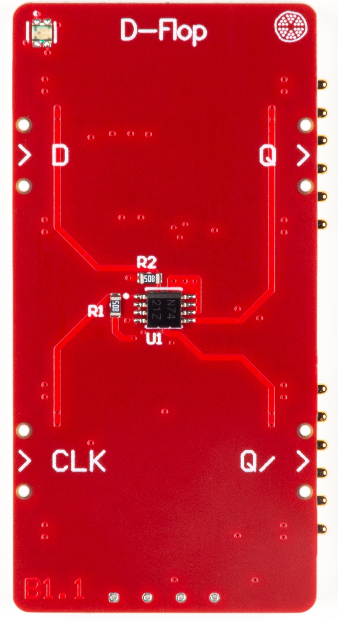
Schematic

Digital Twin
In the PomeLabs App, the PML-DFF-01 is mirrored as a digital twin in both the Playground and inside any Connect Activity. On connection the module reports its unique ID, firmware version, and type, and the App places it in your circuit by reading the live netlist — so you always see which module it is and how it is wired. Its edge-triggered sequential logic runs entirely on the physical hardware; the current release exposes no app-side controls or streamed values for this module.
Datasheet
1. Overview
The PML-DFF-01 implements a single positive-edge-triggered D flip-flop using the SN74LVC1G74DCTR (U1) — Texas Instruments' single-gate D flip-flop with asynchronous active-LOW preset (PRE) and clear (CLR).
On each rising edge of the clock signal (S-_LL → CLK), the logic level present at the data input (S+_LL → D) is captured and transferred to output Q (S+_UR). The complementary output Q̄ (S+_LR) is always the logical inverse of Q. Between clock edges, Q holds its value regardless of changes on D — this is the defining property of edge-triggered storage and the basis of all registers, counters, and state machines.
Asynchronous preset and clear override the clock entirely: asserting PRE LOW forces Q HIGH immediately; asserting CLR LOW forces Q LOW immediately. Both are active-LOW and must be tied HIGH for normal clocked operation.
2. BOM Components
| Ref. | Type | Value / Part | Role on this module |
|---|---|---|---|
| U1 | Single D flip-flop | SN74LVC1G74DCTR (TI) | Positive-edge-triggered D flip-flop. Asynchronous active-LOW PRE and CLR. Both Q and Q̄ outputs. – supply, inputs accept up to . SSOP-8 (DCT) package, body. |
| R1, R2 | Resistor | Pull-up resistors on UART TX/RX lines to . | |
| p1–p4 | Connector | Node headers | Four node connectors exposing , GND, S+, S−, RX/TX, TX/RX. |
3. Electrical Specifications
All values at unless otherwise noted. Flip-flop specifications from TI SCES794G (SN74LVC1G74, Rev. G, Sep 2021).
3.1 U1 — SN74LVC1G74DCTR
3.1.1 Absolute Maximum Ratings
Exceeding these values may permanently damage the device. Stress ratings only.
| Parameter | Max Value | Unit |
|---|---|---|
| Supply voltage () | to | V |
| Input voltage () | to | V |
| Output voltage — high-Z or power-off state () | to | V |
| Output voltage — high or low state () | to | V |
| Input clamp current (), | mA | |
| Output clamp current (), | mA | |
| Continuous output current () | mA | |
| Continuous current through or GND | mA | |
| Package thermal impedance () — DCT package | °C/W | |
| Storage temperature () | to | °C |
3.1.2 Recommended Operating Conditions
| Parameter | Min | Max | Unit / Notes |
|---|---|---|---|
| Supply voltage () — operating | V | ||
| Supply voltage () — data retention only | — | V | |
| Input voltage () | V — inputs tolerant regardless of | ||
| Output voltage () | V | ||
| High-level input voltage () @ to | — | V | |
| Low-level input voltage () @ to | — | V | |
| High-level output current () @ | — | mA — sourcing | |
| Low-level output current () @ | — | mA — sinking | |
| High-level output current () @ | — | mA — sourcing | |
| Low-level output current () @ | — | mA — sinking | |
| Input transition rise/fall rate () @ | — | ns/V | |
| Operating temperature () | °C |
3.1.3 Timing Requirements & Switching Characteristics
At , to , (unless otherwise noted).
| Parameter | Min | Max | Condition |
|---|---|---|---|
| Maximum clock frequency ( / ) | — | MHz | |
| Clock pulse duration (, CLK high or low) | — | ns | |
| PRE or CLR LOW pulse duration () | — | ns | |
| Data setup time (, D before CLK ↑) | — | ns | |
| PRE/CLR inactive setup time (, before CLK ↑) | — | ns | |
| Data hold time (, after CLK ↑) | — | ns | |
| Propagation delay () CLK → Q | — | ns | |
| Propagation delay () CLK → Q̄ | — | ns | |
| Propagation delay () PRE/CLR LOW → Q or Q̄ | — | ns | |
| Propagation delay () CLK → Q @ | — | ns |
Quiescent supply current (): max at or GND, . Input capacitance (): typ at . Power dissipation capacitance (): typ at , .
4. Function Table
Positive-edge-triggered operation. PRE and CLR are asynchronous and active LOW. (Source: TI SCES794G Table 8-1.)
| PRE | CLR | CLK | D | Q | Q̄ | Description |
|---|---|---|---|---|---|---|
| L | H | X | X | H | L | Asynchronous preset — Q forced HIGH regardless of clock |
| H | L | X | X | L | H | Asynchronous clear — Q forced LOW regardless of clock |
| L | L | X | X | H¹ | H¹ | PRE and CLR both asserted — both outputs forced HIGH (nonstable; does not persist when PRE or CLR returns HIGH) |
| H | H | ↑ | H | H | L | Rising edge: D = H captured into Q |
| H | H | ↑ | L | L | H | Rising edge: D = L captured into Q |
| H | H | L | X | Q₀ | Q̄₀ | No clock edge: Q holds previous state |
¹ Per TI SCES794G: this is a nonstable condition rather than strictly forbidden — when one of PRE or CLR is released first, Q resolves to the value driven by the input still asserted. Releasing both simultaneously produces an unpredictable final state.
5. Timing Diagram
Normal clocked operation (PRE = CLR = H):
CLK:  __|‾|___|‾|___|‾|___
D:    _____|‾‾‾‾‾|_______
Q:    _________|‾‾‾‾‾|___   (captured on ↑ edge, held until next ↑ edge)
Q̄:   ‾‾‾‾‾‾‾‾‾|_____|‾‾‾
Asynchronous clear (CLR asserted LOW, independent of CLK):
CLR:  ‾‾‾‾‾|___|‾‾‾‾‾‾‾‾
Q:    ‾‾‾‾‾|_____________   (Q → LOW immediately on CLR↓, no clock needed)
Q̄:   _____|‾‾‾‾‾‾‾‾‾‾‾‾
6. Pin Descriptions
All signal pins are referenced to GND.
| Pin / Net Name | Direction | Description |
|---|---|---|
| S+_LL | Input | Data input D. Logic level captured into Q on the rising edge of CLK. Level between clock edges has no effect. |
| S-_LL | Input | Clock input CLK. Rising edge only is active — captures D into Q. Falling edge and steady state do not change Q. |
| S+_UL | Input | Asynchronous preset (PRE) — active LOW. When LOW: forces Q HIGH and Q̄ LOW immediately, overriding clock. Tie HIGH for normal operation. |
| S-_UL | Input | Asynchronous clear (CLR) — active LOW. When LOW: forces Q LOW and Q̄ HIGH immediately, overriding clock. Tie HIGH for normal operation. |
| S+_UR | Output | Q output. Stored state of the flip-flop. Updates only on CLK rising edge (or asynchronous PRE/CLR). |
| S+_LR | Output | Q̄ output. Always the logical complement of Q. |
| TX_UL-L / TX_LL-L | Input | UART transmit from Backend MCU (USART1/USART3). |
| RX_UL-L / RX_LL-L | Output | UART receive from Upper-Left and Lower-Left connectors. |
| TX_UR-L / TX_LR-L | Input | UART transmit from Backend MCU (USART2/USART4). |
| RX_UR-L / RX_LR-L | Output | UART receive from Upper-Right and Lower-Right connectors. |
| 5V-Module | Power In | supply. Powers of U1. |
| 3V3 | Power In | logic rail for pull-up resistors R1–R2 (). |
| GND | Ground | Common ground for all ICs and connectors. |
7. Connection Guide & Common Errors
Correct power-up sequence:
- Connect GND first, shared across all modules on the common bus.
- Connect 5V-Module to a regulated source to power U1.
- Connect the 3V3 rail for the UART pull-up resistors.
- Drive PRE (S+_UL) and CLR (S-_UL) HIGH before applying any clock — this prevents spurious state changes during power-up. Both inputs must always be at a defined level (HIGH or LOW); never leave them floating.
- Optionally pulse CLR LOW briefly to initialize Q to a known LOW state, then return CLR HIGH.
- Apply the data input on S+_LL (D) and the clock signal on S-_LL (CLK). Q updates on the rising edge of CLK; Q̄ is always the logical inverse.
Logic-level reference at : an input must rise above to register as HIGH and fall below to register as LOW. The flip-flop is level-triggered on the clock pin (any input crossing from below counts as a rising edge), so clean, fast clock edges are recommended even though the device does not require a specific rise time.
Common wiring errors and consequences:
| Mistake | Symptom | Correction |
|---|---|---|
| PRE (S+_UL) or CLR (S-_UL) left floating | Floating CMOS input drifts; the asynchronous override may assert at random and toggle Q without a clock edge | Always drive both PRE and CLR HIGH (e.g. through a pull-up to 3V3 or a logic HIGH source) when not actively asserting them. Never leave them floating. |
| PRE and CLR both asserted LOW simultaneously | Both Q and Q̄ are driven HIGH — a nonstable condition; the final state when they release is unpredictable if released at the same instant | Avoid asserting PRE and CLR together. If unavoidable, ensure one is released cleanly before the other so the flip-flop settles to the corresponding defined state. |
| D (S+_LL) changes within the setup/hold window around CLK ↑ | Setup/hold violation — the flip-flop can enter a metastable state; Q may take an unbounded time to resolve to a valid logic level | Keep D stable for at least before and after the CLK rising edge (at ). |
| Clock pulse too narrow (high or low time below ) | The flip-flop may fail to register the edge, or the new Q value may not propagate cleanly | Keep both the HIGH and LOW phases of CLK at least wide at ( at ). |
| Clock frequency exceeds | Q fails to capture D correctly — missed transitions, glitches | Keep CLK below at or at (per TI SCES794G). Use a flip-flop chain or pipeline at higher frequencies. |
| Very slow input edges (slower than at ) | Operation outside the guaranteed input transition rate; CLK in particular may produce double-clocking or unstable Q | Drive CLK from a logic-level source (or a debounced/Schmitt-buffered button). Buffer slow analog-like signals before feeding them to D or CLK. |
| to U1 exceeds | U1 permanently damaged (absolute max ) | Keep the 5V-Module rail . |
| Input signal on D, CLK, PRE, or CLR exceeds | Input clamp current flows; permanent damage if exceeds | Inputs are tolerant — never exceed it. Add a series resistor if your source can swing higher. |
| Output Q or Q̄ driving load | Continuous output current absolute max exceeded — U1 may overheat or fail | Keep on each output within absolute max. For sustained operation, design for at or at . |
| Powering D, CLK, PRE, or CLR while 5V-Module is OFF | circuitry isolates U1 and prevents back-drive damage — designed-in safe condition, not a fault | No action needed; partial-power-down via is supported by the device. |
How is this guide?